
In many industrial sectors, the optimisation of materials and manufacturing processes relies on in-depth knowledge of the microstructure and crystallographic properties of materials. EBSD analysis (Electron Backscatter Diffraction) is proving to be a cutting-edge technique for addressing a wide range of complex issues.
As a manufacturer, would you like to carry out an EBSD SEM analysis?
What is Scanning Electron Microscopy EBSD (SEM-EBSD)?
Scanning Electron Microscopy (SEM) coupled with Electron Backscatter Diffraction (EBSD) is a state-of-the-art technique used in the laboratory to analyze the crystalline microstructure of materials. This method combines the high-resolution imaging capability of SEM with the detailed analysis of crystal structure and texture via EBSD.
SEM-EBSD reveals precise information on crystal orientation, grain boundaries, crystalline phases and structural deformations. These data are important for understanding how microstructure influences the mechanical and physical properties of materials.
EBSD (Electron BackScatter) is a backscattered electron diffraction imaging mode that can be combined with SEM. EBSD is a technique for analysing the internal structure of materials (microstructure).
> EBSD provides information on crystal orientation and grain structure at the micrometre and even nanometre scales, giving a detailed understanding of the microstructure.
> This technique can map the texture of a material, revealing how grains are oriented relative to each other, in order to understand the mechanical properties of materials.
> EBSD analysis can identify the different crystalline phases present in a sample and their distribution, which is essential for multiphase materials.
> EBSD can reveal the presence of crystalline deformations, dislocations and other structural defects, providing valuable information for materials engineering and materials science research.
Why carry out an EBSD SEM analysis in the laboratory?
Performing EBSD-MEB analysis in the laboratory helps to decipher the microstructure of materials, optimise manufacturing processes and ensure quality control in a variety of sectors.
This advanced analysis technique reveals precise details of grain size, orientation and grain boundaries, making it possible to improve material properties such as strength, ductility and reliability.
SEM EBSD analysis is also used in the development of new materials and the understanding of deformation and ageing mechanisms.
Our solutions: offer EBSD SEM analysis techniques specific to your requirements and determine the microstructure of your material
SEM EBSD analysis, a state-of-the-art technical tool
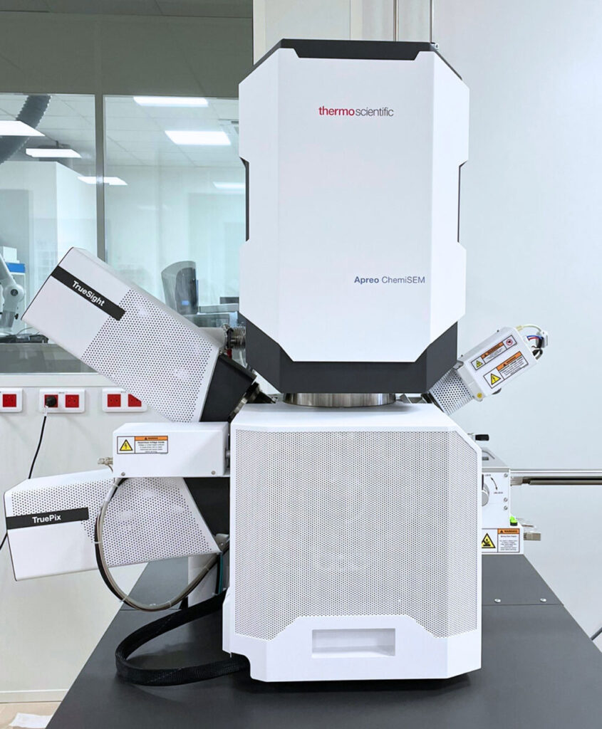
As a meb ebsd analysis laboratory, FILAB is now one of the first French laboratories to be equipped with the Zeiss GEMINI SEM… SEM-EDX-EBSD. This microscopic SEM analysis tool is particularly powerful and efficient for rapid diagnosis (pollution, inclusion, etc.) or more complex expert assessments.
The SEM EBSD analysis technique is based on the use of an incident electron beam of a few tens of kilovolts sweeping across the surface of the sample, which then re-emits a whole spectrum of particles and radiation: secondary electrons, backscattered electrons, Auger electrons or even X-rays.
The electron beam is produced in an ‘electron gun’ and then directed through a set of electromagnetic lenses and scanning coils that form the SEM column.
Our EBSD SEM analysis services
Inspecting for failure
Identification of particles, contaminants and deposits
Surface layer analysis
Nanometric characterization: FILAB is the first French laboratory to be COFRAC ISO 17025 accredited in this field
Surface analysis
SEM-EBSD: what can you do with this technique?
By combining SEM and EBSD data with complementary techniques such as EDX (analysis by X-ray spectrometry), it is possible to obtain precise chemical and mineralogical mapping. This multi-dimensional approach helps to understand corrosion, contamination and failure mechanisms in materials.
For manufacturers, controlling the dimensions and shapes of particles or internal structures is extremely important. SEM can be used to measure the dimensions, coating thickness and pores of materials with nanometric precision. This data is essential for guaranteeing the quality and performance of end products.
Thanks to the magnification and resolution capabilities of the SEM, manufacturers can identify and analyse defects in their materials or products. Cracks, inclusions, gas bubbles or delaminations: these observations can be used to diagnose and correct sources of failure. The addition of EBSD makes it possible to analyse the impact of crystalline orientations or internal stresses on these defects.
Industrial applications of the SEM EBSD analysis technique
Scanning Electron Microscopy-Electron Backscatter Diffraction (SEM-EBSD) has applications in a variety of industries thanks to its ability to provide detailed information on the microstructure of materials.
In the metallurgical industry, SEM-EBSD is used to analyse the structure of metal alloys, optimise heat treatments and understand deformation and fracture mechanisms. It helps to improve the quality and mechanical properties of finished products such as steel and aluminium.
In the microelectronics and semiconductor industries, this technique is used to examine crystallinity and defects in semiconductor materials such as silicon and germanium. EBSD analysis can be used to optimise manufacturing processes and improve the performance and reliability of electronic devices.
For composite materials, EBSD can be used to study the orientation of fibres and reinforcements in matrices, in order to design materials with optimised mechanical properties for specific applications, such as carbon fibre-reinforced polymer matrix composites used in aerospace.
For the energy sector, particularly in the development of materials for nuclear energy, meb ebsd analysis helps to determine the structure of irradiated materials and to understand their behaviour under irradiation. This makes it possible to develop more resistant materials for nuclear reactors, thereby improving safety and energy efficiency.
Problems solved by EBSD for industry
EBSD analysis is particularly useful for applications such as :
- Validation of welding or brazing processes: EBSD can be used to assess the crystalline orientations of welded joints and detect any critical areas that could cause mechanical failure of the assemblies.
- Analysis of wear and friction mechanisms: by identifying the microstructures responsible for damage or fatigue, it is possible to optimise the design of parts and increase their durability.
- Characterization of phase transformations: essential for complex metal alloys, EBSD makes it possible to monitor and optimise microstructural changes during heat or mechanical treatments.
- Monitoring intragranular gradients: by studying the internal orientations of grains, it is possible to better understand the effects of mechanical treatments such as rolling or plastic deformation.
- Optimisation of surface treatments: EBSD helps to assess the effectiveness of coatings or heat treatments in terms of adhesion, corrosion resistance or overall performance. This evaluation can also be done by electrochemical tests
- Advanced applications for innovative materials: EBSD is also essential in the development and validation of new-generation materials.
FAQ
A meb ebsd analysis can provide detailed information on various elements and properties of materials, including the following:
- Crystal orientation and texture: details of the specific and preferential orientation of crystals and grains in a material.
- Grain size: measurement of the average size of the crystalline grains present.
- Grain boundaries: identification of the boundaries between different crystalline grains.
- Crystalline phases: identification of the different crystalline phases present in the sample.
- Crystalline deformations: details of the deformations undergone by the crystalline structure (stretching, compression).
- Crystal defects: information on defects in the crystal structure (dislocations, grain boundaries)
- Internal and mechanical stresses: measurement of the mechanical stresses present inside the material, and deformation behaviour under load (hardness, resilience).
This information is important for materials research and development, enabling the mechanical, chemical and physical properties of materials to be optimised for specific applications.
The ebsd meb is generally used to study the 3D morphology with nanometric resolution of the surface of an object or material. Chemical and elemental composition can also be obtained by X-ray microanalysis.
It can be used to provide a range of images:
- Topographical imaging, which provides a topographical view of the sample by detecting secondary electrons.
- Chemical imaging, which shows the chemical composition by electron contrast.
- X-ray microanalysis for elemental analysis of the sample
SEM-EBSD analysis provides detailed results in the form of microstructural and crystallographic maps, showing grain orientations, phases present, grain boundaries and intragranular orientation gradients. These results also include quantitative data such as crystallographic texture (preferential orientation), phase volume fraction and grain size and distribution. This information helps to understand deformation mechanisms, optimise industrial processes and ensure that materials comply with current standards.
EBSD offers local, spatially resolved analysis, unlike XRD, which provides global data. It allows precise mapping of crystallographic orientations, grain boundaries and phases, ideal for studying local heterogeneities or complex microstructures. Coupled with SEM, it provides detailed imaging and complementary chemical data, essential for specific problems such as defect analysis or treatment optimisation.
EBSD is used to analyse the microstructures of welded or brazed joints. It identifies crystallographic orientations, areas of recrystallisation or brittle phases likely to compromise the strength of the assembly. This analysis helps to optimise process parameters to reduce cracks, porosity and structural heterogeneity, thereby ensuring greater weld reliability.
By studying the microstructure of surfaces and internal layers, EBSD detects wear mechanisms, such as the alteration of crystallographic orientations or the formation of specific textures in mechanically stressed areas. This information can be used to adapt materials, heat treatments or coatings to improve friction resistance and extend the life of parts.
Yes, EBSD is a method for monitoring and quantifying phase transformations induced by thermal or mechanical treatments. For example, it can detect phase changes in complex alloys, helping to optimise manufacturing processes such as forging, rolling or thermal hardening.
EBSD can be used to assess the effects of surface treatments, such as coatings or thermochemical treatments, by analysing the microstructure and crystalline orientations. The technique helps to measure layer uniformity, adhesion and corrosion resistance, providing accurate validation to ensure surface performance.
EBSD is capable of characterising small-scale structures, such as nanoparticles or thin films, by identifying their phases and crystallographic orientations. This analysis is commonplace in high-tech industries, particularly in the development of materials for electronics, energy and optics.
A SEM-EBSD analysis laboratory offers cutting-edge expertise and high-precision equipment for studying the microstructures of materials. FILAB gives manufacturers access to detailed data on crystallographic orientations, phases and microstructural properties, which are essential for solving complex problems such as the optimisation of manufacturing processes, failure analysis and the development of new materials.


