The Story of a Scientific Discovery: The Scanning Electron Microscope
Scanning Electron Microscope (SEM): what is it?
The Scanning Electron Microscope (SEM) is a characterization technique that produces high-resolution images of a sample’s surface. Using the principle of electron-matter interactions, SEM offers much better resolution than traditional optical microscopes, which are limited by the wavelength of visible light and the quality of optical lenses.
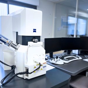
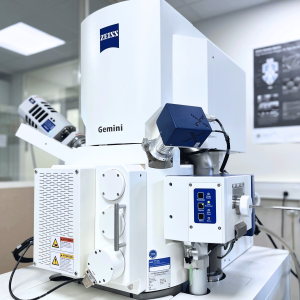
An SEM consists of an electron column, an electron gun (an electron gun used to strike the surface of the sample), detectors, and a stage for moving the object to be analyzed.
This device is now used in many industrial fields to analyze the surface properties of a material or to characterize a defect or contamination (particle, deposit, crack, etc.).
A story that began in the early 1930s...
The first work on the design of an electronic optical device began in Germany. In the early 1930s, Max Knoll developed an electron beam analyzer, which he incorporated into what was the first transmission electron microscope.
A few years later, scientist Manfred Von Ardenne completed this work by adding scanning coils: in 1938, he built the first Scanning Electron Microscope.
It was in England, specifically at the University of Cambridge, that the history of SEM continued. In the late 1940s, Charles Oatley and Dennis McMullan succeeded in obtaining a relief image, a feature of “modern” SEMs. This breakthrough was complemented by the work of T.E. Everhart and R.F.M. Thornley, which led to a new detector capable of detecting secondary electrons.
Very quickly, the first MEB prototypes were installed in the 1960s in Germany, England, and France.
New modern applications of SEM
Since then, numerous innovations have expanded the performance and areas of application of the scanning electron microscope. Here are a few examples:
- Digital SEM integrating manual control and direct scanning
- Dual column SEM (FIB)
- High-resolution SEM (FEG) allowing magnifications of around 100,000 to be achieved. 3D and color imaging have also contributed to greater accuracy and improved readability.
- SEM EDS/EDX, for chemical diagnostics (semi-quantitative elemental analysis)
- Environmental scanning electron microscope (ESEM) including controlled pressure modes for low-conductivity samples (particularly glass or plastic).
- SEM EBSD, for characterizing microstructures and crystallographic properties
Take advantage of our analysis services and the performance of our latest-generation MEB-FEG EDX and MEB-EBSD systems.
Our laboratory has two SEM-FEGs coupled with an EDX probe and one SEM-FEG coupled with an EBSD probe in order to broaden our field of expertise and achieve a higher level of extreme surface characterization for services such as:
- Identification of chemical nature
- Control of thin-film treatments
- Pollution detection
- The search for inclusion
- Failure expertise
- Analysis of issues related to delamination or lack of adhesion


