Traveling into the infinitely small… AFM at the service of extreme surfaces
What are the modes and applications of AFM?
FILAB laboratory is pleased to announce the arrival of AFM at its analytical facility in Dijon in early September 2022. It has been equipped with an FX40 Automatic AFM, which is equipped with AI. It enables faster and more reliable analysis. This makes FILAB the first laboratory in Europe to be equipped with an AI-powered AFM.
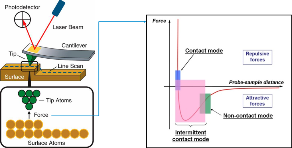
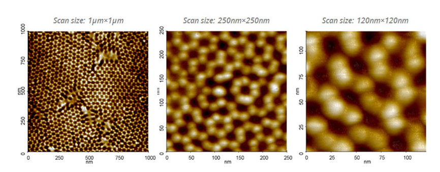
The Atomic Force Microscope is a high-resolution local probe microscope that can be used to visualize the topography of a sample’s surface as well as its tribology, mechanical behavior, electrical behavior, and chemical behavior.
This method allows for point-by-point analysis of the sample surface using a probe consisting of a nanometric tip. This microscope therefore offers the possibility of studying the infinitely small.
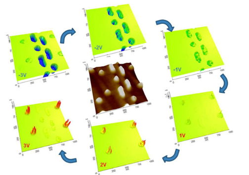
Depending on the problem encountered, AFM offers several modes: contact mode and non-contact mode. But then, which modes are used for which applications?
The mode
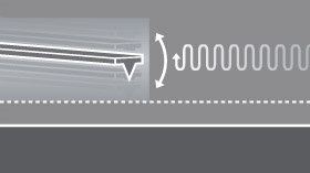
non-contact
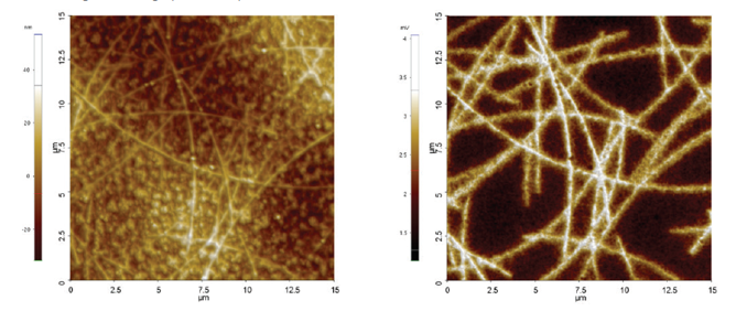
The non-contact mode of the AFM allows the topography of the sample to be measured without damaging it.
The mode
contact
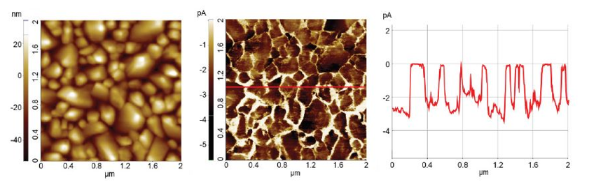
As for the AFM’s contact mode, it also allows the topography to be measured (although this is less commonly used) but above all to perform various measurements:
mechanical
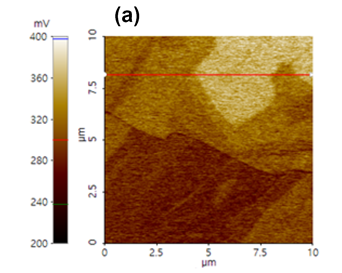
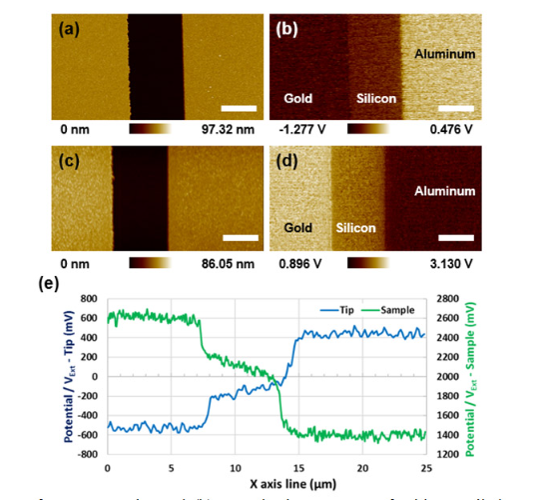
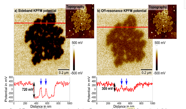
electrical
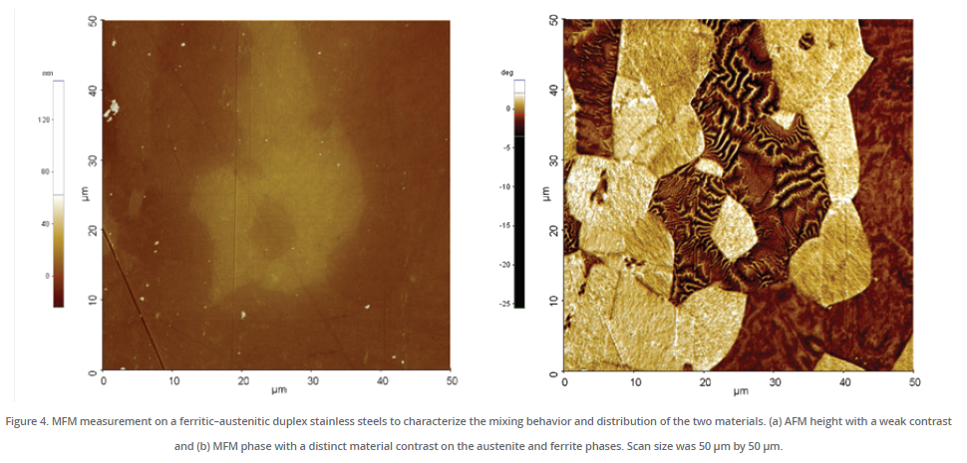
magnetic
To do this, it is necessary to adapt the type of tip according to the sample (stiffness constant and application).
Discover the different ways to contact the AFM:
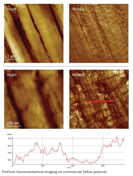
FMM mechanical mode
Among all contact modes, the FMM mechanical mode allows measurements of mechanical properties (Young’s modulus, deformation, adhesion) to be taken.
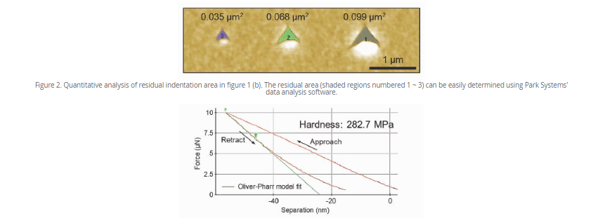
Mechanical nanoindentation mode
Mechanical nanoindentation mode, meanwhile, allows various measurements to be taken:
Hardness measurements and Young’s modulus
Indentation area measurements to calculate hardness
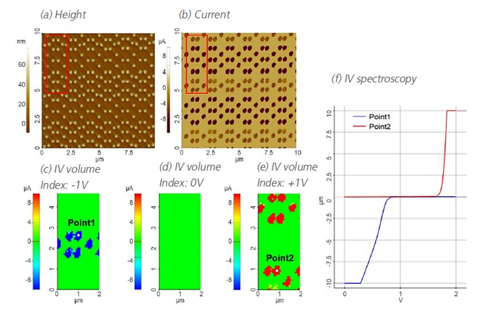
C-AFM pinpoint electric mode
With the C-AFM pinpoint electric mode, it allows you to: