
What is Atomic Force Microscopy (AFM)?
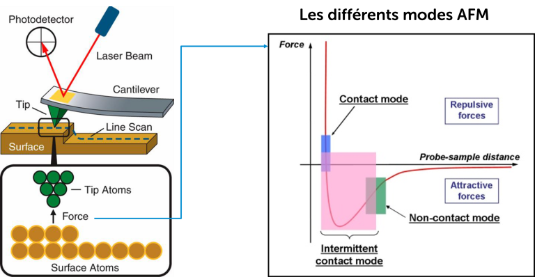
The Atomic Force Microscope (AFM) is a microscope with a local probe, high resolution to visualize the topography of the surface of a sample but also the tribology, the mechanical, electrical or chemical behavior.
Indeed, the very principle of microscopic study is to rely on light. However, once in the universe of the infinitely small (less than a few hundred nanometers), the observation conditioned to light becomes impossible since the limit of resolution is about 100µm.
AFM allows to overcome these limits since this type of microscopy works by measuring the attractive or repulsive interactions between the tip of the AFM and the surface of the sample.
The FILAB laboratory has cutting-edge AFM equipment for the analysis of surfaces and in particular the characterization of nanomaterials.
FILAB laboratory analysis the surfaces of your samples by AFM
The FILAB laboratory specializing in surface analysis provides you with a cutting-edge technique: AFM (Atomic Force Microscopy). This technique allows a fine and precise analysis of the surfaces of your samples, revealing details invisible to the naked eye.
Our AFM laboratory offers comprehensive AFM testing and analysis services, enabling detailed characterization of surface topography, roughness, and mechanical properties at the nanoscale.
With our state-of-the-art equipment, we provide accurate and reliable AFM characterization for various materials, ensuring high-resolution imaging and precise measurements. Our expertise in atomic force microscopy analysis allows us to support research and development projects across multiple industries.
Capabilities and Services
The different configurations
AFM: to characterize all types of materials, measure roughness (MDR context), elasticity, adhesion, friction and surface energy...
SMM: Scanning Microwave Microscopy is an AFM coupled to microwave spectroscopy. The tip serves as a local microwave (gigahertz) transmitter and receiver, enabling non-destructive topographic and tomographic analysis while retaining the essential property of AFM: nanometric resolution. SMM can be used to characterize all types of materials, measure microstructural changes, identify the presence of buried defects, measure sub-surface mechanical stresses, determine diffusion profiles for light elements (oxygen, nitrogen and even hydrogen!), all while being non-destructive... It's a revolution!
The UA-AFM is an AFM coupled with acoustic spectroscopy. Based on the same principle as ultrasound, it enables tomography at nanometric and micrometric scales to characterize all types of materials, while being non-destructive like MMS. Sensitive to density variations, it enables 3d reconstruction of the first few micrometers of a surface to identify inclusions, defects that may be a source of corrosion or fracture...
IR-AFM: is an AFM coupled to infrared spectroscopy. This technique, based on the photothermal effect induced by laser illumination, enables chemical mapping of the surface with nanometric resolution.
Our AFM testing services include:
High-resolution imaging of surface morphology
Assessment of mechanical properties such as stiffness and elasticity
Surface energy analysis for material compatibility studies
These capabilities enable us to perform thorough AFM analysis tailored to your specific requirements
Quantitative measurements of surface roughness and texture
Evaluation of adhesion and friction forces
Applications
Our AFM laboratory supports a wide range of applications, including:
Material science research for nanostructure analysis
Failure analysis of coatings and thin films
Quality control in manufacturing processes
Surface modification studies for improved material performance.
Example of services by AFM
Search for mechanical constraints that could be the cause of a fracture
Search for conductivity or electrical permittivity defects (semiconductor)
Measurement of non-destructive deposit thickness on the surface of a part
Profil de diffusion d’éléments légers (oxygène, azote, hydrogène…) en mode non destructif (équivalent à la NRA)
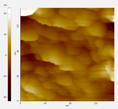
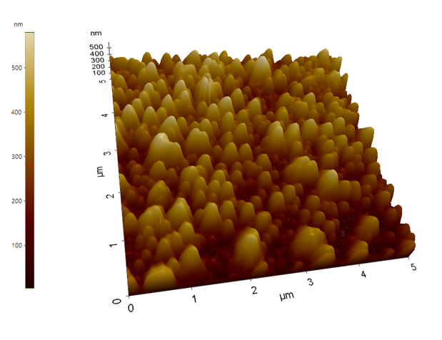
Characterization of nanostructures by AFM measurement
Comparative study of AFM vs SEM surface
Search for buried defects (inclusions, crystallization defects, etc.)
Tomography with nanometer resolution
Local mechanical measurement in the context of non-compliance or part inspection
Verification of the homogeneity of a deposit or surface functionalization
Characterization of surface properties
Examples of matrices to be analyzed by AFM
Why Choose FILAB for AFM Services?
FILAB stands out as a premier AFM laboratory thanks to several key strengths.,
Our team of experienced scientists specializes in atomic force microscopy (AFM) analysis, bringing deep expertise to every project.
Each testing protocol is customized to meet the unique needs of our clients, ensuring relevant and reliable results. We are committed to delivering comprehensive reports that include actionable insights.
By choosing our AFM testing services, you benefit from our dedication to excellence and precision in every aspect of atomic force microscopy analysis.
The AFM microscope, cutting-edge equipment
Industry is a field that requires flawless precision. This is why the power of an AFM microscope is necessary for certain industrial applications. Indeed, visualizing structures at the nanoscale can be used to inspect materials, identify surface defects, and even understand how individual molecules interact.
The advantages of analysis by AFM (Atomic Force Microscopy)
The advantages of an AFM microscope are numerous. This type of microscope allows more precise visualization of surfaces at the nanoscale, thus providing better analysis of the structure of the material.
Additionally, AFM also allows measuring surface forces such as adhesion or repulsion force, a parameter often considered in the manufacturing or development of new materials.
The different types of probes that can be used on the AFM
One of the common operating techniques of AFM that provides high-resolution images of the surface topography of a sample. In this mode, the cantilever point is in constant contact with the sample.
Also known as intermittent contact mode. In this mode the cantilever tip does not come into contact with the sample. The tip is oscillated near its resonant frequency and scans the sample surface with a constant amplitude. The force variations recorded are used to create a topographic image of the surface under study.
These two application modes are advanced AFM techniques. They combine the advantages of force spectroscopy and tapping. The cantilever tip does not come into contact with the sample, it is set in modulated oscillation at a lower frequency than in the traditional tapping mode. The force exerted on the sample is measured at each scanning point, thus allowing the mapping of the mechanical properties of the surface at the nanometric scale.
The QNM mode extends this analysis by allowing a quantitative mapping of the observed mechanical properties.
With this mode of application of AFM it is possible to map the electrical conductivity of the surface of materials at the nanometric scale. A small electric current diffused in the tip of the cantilever scans the surface of the sample and at each point the electrical conductivity is measured.
It allows mapping of electrical capacitance variations at the nanoscale on the surface of a sample. A probe tip is placed close to the surface of a sample, forming a capacitor. Electrical capacitance is measured by applying an alternating voltage to the tip and measuring the resulting alternating current.
This technique measures and maps electrical resistance variations at the nanoscale on the surface of a sample. A conductive probe tip is placed on the surface of a sample. The electrical resistance is measured as a function of the voltage applied as the tip scans the sample.
It allows the study of cracking or deformation of the surface of a coating.
FAQ
AFM testing is used to analyze surface properties such as roughness, texture, adhesion, elasticity, and mechanical resistance at the nanoscale.
AFM analysis is suitable for a wide range of samples including metals, polymers, ceramics, biological tissues, thin films, and coatings.
While both techniques provide surface imaging, AFM uses a physical probe to scan surfaces, offering higher resolution for surface texture and mechanical property mapping.
SEM uses electron beams and is better for overall morphology at high speed.
Industries such as medical devices, electronics, aerospace, automotive, and pharmaceuticals benefit from AFM testing to control quality, ensure compliance, and support R&D.


