
The filab advantages

A highly qualified team

Responsiveness in responding to and processing requests

A COFRAC ISO 17025 accredited laboratory
(Staves available on www.cofrac.com - Accreditation number: 1-1793)

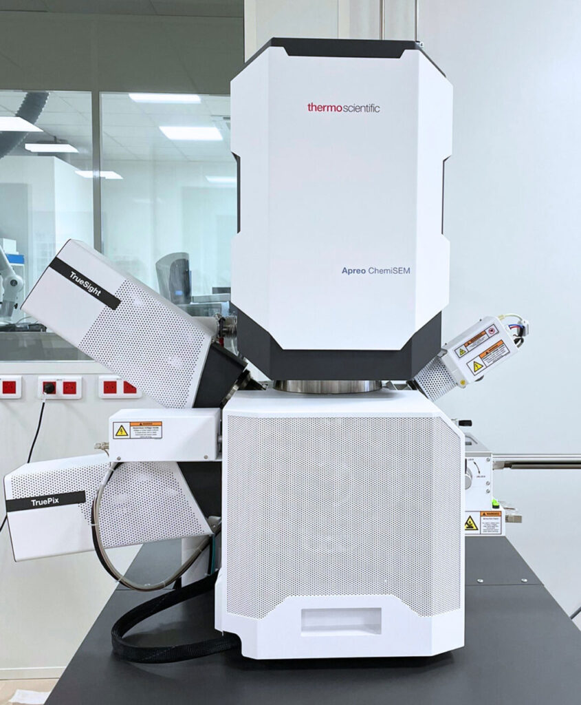
A complete analytical facility of 5,200m²

Tailor-made support

Video debriefing available with the expert


Ask for your quote