


SEM-EBSD: as an industrial professional, do you want to carry out an EBSD analysis?
What is scanning electron microscopy EBSD (SEM-EBSD)?
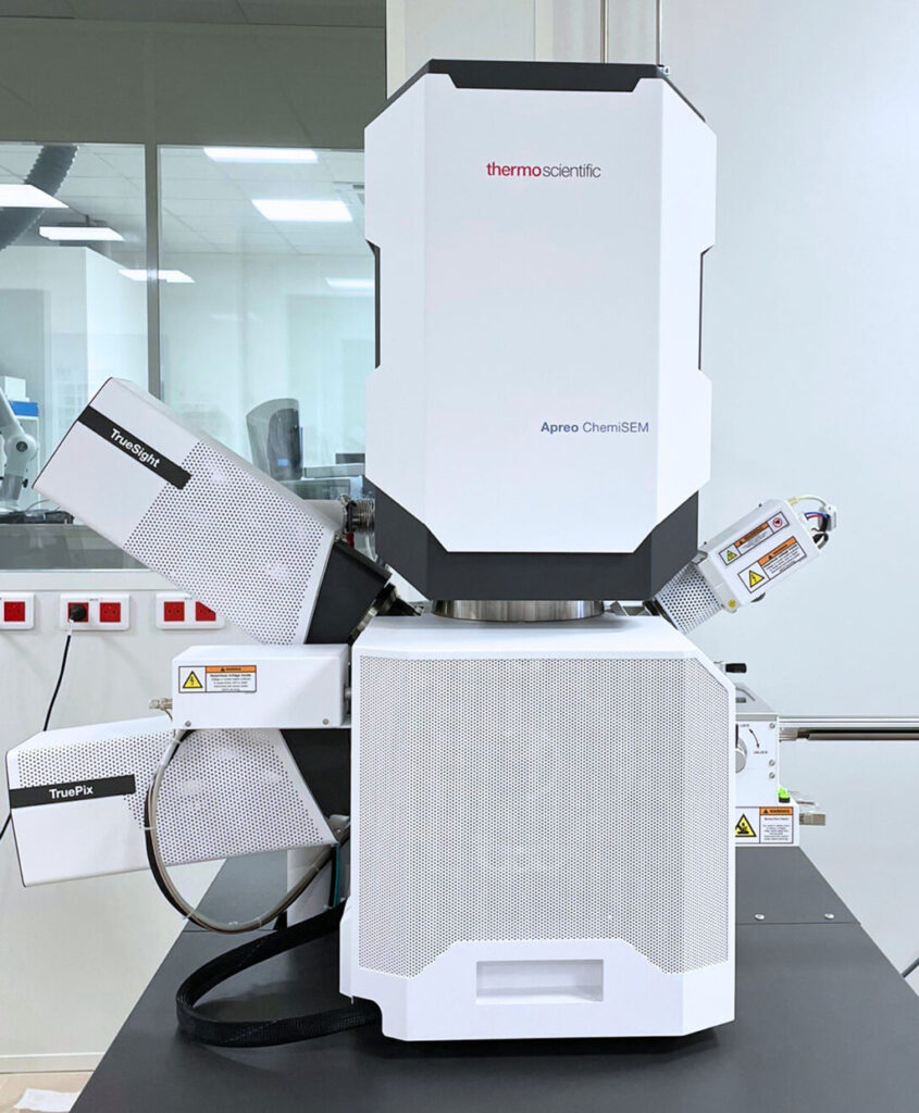
Scanning Electron Microscopy (SEM) combined with Electron Backscatter Diffraction (EBSD) is a cutting-edge technique used in laboratories to analyze the microstructure of crystalline materials. This method combines the high-resolution imaging capability of SEM with detailed analysis of crystal structure and texture via EBSD.
As a SEM EBSD analysis laboratory, FILAB is now one of the first French laboratories to be equipped with the MEB-EDX-EBSD GEMINI SEM model from Zeiss. This SEM microscopic analysis tool is particularly powerful and efficient for rapid diagnostics (contamination, inclusion, etc.) or more complex expert assessments.
By choosing FILAB’s EBSD analysis, you benefit from recognized expertise and precise results, tailored to the requirements of your industrial sector.
Industrial applications of the SEM EBSD analysis technique
EBSD analysis is essential for industrial professionals looking to assess the microstructure, texture, and residual stresses of metallic, ceramic, or polymeric materials.
By combining SEM and EBSD data with complementary techniques such as EDX (X-ray spectrometry analysis), it is possible to obtain precise chemical and mineralogical mapping. This multidimensional approach helps to understand corrosion phenomena, contamination, and even failure mechanisms in materials.
For industrial professionals, controlling the dimensions and shapes of particles or internal structures is essential. SEM makes it possible to measure dimensions, coating thickness, and even material pores with nanometric precision. These data are essential to ensure the quality and performance of final products.
Thanks to the magnification and resolution capabilities of SEM, industrial professionals can identify and analyze defects present in their materials or products. Cracks, inclusions, gas bubbles, or delaminations: these observations make it possible to diagnose and correct the sources of failure. Adding EBSD makes it possible to analyze the impact of crystal orientations or internal stresses on these defects.
FILAB offers you a funnel strategy to precisely identify your material by relying on SEM-EBSD as well as other complementary techniques.
- Chemical composition study by SEM-EBDX and ICP-AES
- Study of crystalline phases by XRD and EBSD
- Study of microstructures and orientations by EBSD
SEM-EBSD applications by sector
The problem: 3D-printed parts can show unexpected weaknesses.
The EBSD solution: Analyze grain orientation along the laser cooling axis. This makes it possible to adjust printing parameters to ensure that a turbine blade will perfectly withstand flight stresses.
The problem: Controlling the quality of a multiphase steel (e.g., Dual Phase steel for the automotive industry).
The EBSD+EDX solution: Simultaneously map the carbon distribution (EDX) and distinguish austenite from martensite (EBSD) to validate that the heat treatment has worked perfectly, thereby ensuring the strength of the chassis.
The problem: invisible micro-cracks cause failures in integrated circuits.
The EBSD solution: measure micro-strains and stresses at grain boundaries in copper or tin solder joints, in order to prevent failures caused by thermal fatigue.
Sample preparation for MEB-EBSD: FILAB at the service of your analysis
Mechanical polishing
For the study of particle size distribution, the identification of crystalline phases, or the determination of the overall grain orientation, mechanical polishing is essential.
Thanks to a controlled protocol, our teams prepare your samples to provide a flat, clean surface, perfectly suited to standard microstructural mapping, while guaranteeing a fast and controlled process.
FIB preparation
When your objectives require fine analysis such as measuring permanent deformation, studying twins, or mapping microstresses, mechanical polishing is no longer enough.
FILAB offers FIB preparation (Focused Ion Beam): this cutting-edge technology removes the work-hardened surface layer to preserve the material’s native crystalline state, thereby unlocking the full power of EBSD.
Not sure which preparation is right for your material? Contact our experts to define the ideal protocol according to your analysis objectives.
MEB-EBSD analysis services by FILAB laboratory
Custom sample preparation
Standard analysis area: typical maps of 1 x 1 mm² or 500 x 500 µm
Measured indicators:
- Grain size: grain size, shape and distribution
- Crystal orientation: preferred grain orientation direction
- Phase analysis: qualitative/quantitative identification of the matrix, precipitates and intermetallic compounds (IMC)
- Crystallographic texture: pole figures and MUD index of the matrix
- Strain mapping: qualitative mapping of permanent strain (intragranular misorientation fields and lattice strain)
Data processing & expert report
Our additional services
Failure analysis expertise
The identification of particles, contaminants and deposits
Contaminant and particle
analysisNanometric characterization : FILAB is also the first French laboratory to be COFRAC ISO 17025 accredited in this field
The analysis of surfaces
Surface layer analysis
What is EBSD analysis?
Thanks to EBSD analysis, it is possible to map the distribution of crystalline phases in a material, providing a detailed view of its microstructure. It is an imaging technique used to obtain information on:
- Crystal orientation and grain structure.
- Material texture, revealing grain alignment.
- Crystalline phases and their distribution, essential for multiphase materials.
- Structural defects (deformation, dislocations).
Benefits of EBSD analysis
EBSD is particularly used for the analysis of polycrystalline materials, such as metals, ceramics, and alloys, and is essential for the microstructural characterization of industrial materials.
Crystallographic precision : This technique provides detailed information on crystal structure and grain orientation, with high resolution
Quantitative analysis : EBSD makes it possible to measure grain size, crystallographic texture, and dislocation density, providing accurate, actionable data
Wide range of applications : The technique is suited to studies of plastic deformation, crystal orientation, and microstructural evolution in various industrial sectors
Phase mapping : It makes it possible to map the different crystalline phases on the same surface, thereby identifying heterogeneities
Fast turnaround : Thanks to integration with modern SEMs, EBSD analysis are fast and make it possible to process a large number of samples
Industrial challenges solved by EBSD
EBSD analysis is particularly useful for applications such as:
EBSD makes it possible to assess crystal orientations at welded joints and detect any critical areas that could lead to mechanical failure of assemblies.
By identifying the microstructures responsible for damage or fatigue, it becomes possible to optimize part design and increase their durability.
Essential for complex metal alloys, EBSD makes it possible to monitor and optimize microstructural changes during thermal or mechanical treatments.
By studying the internal orientations of grains, it is possible to better understand the effects of mechanical treatments such as rolling or plastic deformation.
EBSD helps assess the effectiveness of coatings or heat treatments in terms of adhesion, corrosion resistance, or overall performance. This assessment can also be carried out through electrochemical tests.
EBSD is also essential in the development and validation of next-generation materials.
FAQ
If MEB-EDX tells you what your material looks like (topography) and what it is made of (chemistry), adding an EBSD detector (Electron Backscatter Diffraction) reveals how it is structured.
It is the ultimate tool for understanding the crystallography of your samples and directly linking their microstructure to their mechanical or physical properties.
An SEM-EBSD analysis laboratory offers in-depth expertise and high-precision equipment for studying material microstructures. FILAB enables manufacturers to access detailed data on crystallographic orientations, phases, and microstructural properties, which are essential for solving complex issues such as process optimization, failure analysis, and the development of new materials.
EBSD provides local, spatially resolved analysis, unlike XRD, which delivers global data. It makes it possible to map crystallographic orientations, grain boundaries, and phases with precision, making it ideal for studying local heterogeneities or complex microstructures. Combined with SEM, it provides detailed imaging and complementary chemical data, essential for specific issues such as defect analysis or process optimization.
For an unknown material, we support you through a methodical 3-step approach:
- ICP / MEB-EDX: determination of the overall and local chemical composition
- XRD (X-ray Diffraction): prior identification of the crystalline phases present (an essential step for setting up and calibrating EBSD).
- MEB-EBSD: microstructure mapping and grain orientation analysis
Une analyse meb ebsd peut fournir des informations détaillées sur divers éléments et propriétés des matériaux, notamment les éléments suivants :
- Orientation cristalline et texture : détails sur l'orientation spécifique et préférentielle des cristaux et grains dans un matériau.
- Taille des grains : mesure de la taille moyenne des grains cristallins présents.
- Limites de grains : identification des frontières entre les différents grains cristallins.
- Phases cristallines : identification des différentes phases cristallines présentes dans l'échantillon.
- Déformations cristallines : détails sur les déformations subies par la structure cristalline (étirements, compressions)
- Défauts cristallins : information sur les défauts dans la structure cristalline (dislocations, joints de grains)
- Contraintes internes et mécaniques : mesure des contraintes mécaniques présentes à l'intérieur du matériau, et des comportement de déformation sous charge (dureté, résilience)
Ces informations sont importantes pour la recherche et le développement de matériaux, permettant d'optimiser les propriétés mécaniques, chimiques, et physiques des matériaux pour des applications spécifiques.
SEM EBSD is generally used to study the 3D morphology of the surface of an object or material with nanometric resolution. Chemical and elemental composition can also be obtained by X-ray microanalysis.
Its use makes it possible to provide different images:
- Topographic imaging, which provides a topographic view of the sample through secondary electron detection.
- Chemical imaging, which makes it possible to visualize chemical composition through electron contrast
- X-ray microanalysis, which enables elemental analysis of the sample
Yes, EBSD is a method that makes it possible to track and quantify phase transformationsinduced by thermal or mechanical treatments. For example, it can detect phase changes in complex alloys, helping to optimize manufacturing processes such as forging, rolling, or heat hardening.
EBSD makes it possible to analyze microstructures at welded or brazed joints. It identifies crystallographic orientations, recrystallized areas, or brittle phases likely to compromise the strength of the assembly. This analysis helps optimize process parameters to reduce cracks, porosity, and structural heterogeneities, thereby ensuring better weld reliability.
By studying the microstructure of surfaces and internal layers, EBSD detects wear mechanisms such as changes in crystallographic orientations or the formation of specific textures in mechanically stressed areas. This information makes it possible to adapt materials, heat treatments, or coatings to improve friction resistance and extend the service life of parts.
EBSD makes it possible to evaluate the effects of surface treatments, such as coatings or thermochemical treatments, by analyzing microstructure and crystal orientations. This technique helps measure layer uniformity, adhesion, and corrosion resistance, providing precise validation to ensure surface performance.
EBSD is capable of characterizing small-scale structures, such as nanoparticles or thin films, by identifying their phases and crystallographic orientations. This analysis is common in high-tech industries, particularly in the development of materials for electronics, energy, or optics.
EBSD is an extremely surface-sensitive analysis technique (a few tens of nanometers deep).
The slightest surface alteration during preparation, such as work hardening caused by overly aggressive polishing, can mask diffraction patterns and distort the analysis.
Contact the engineers at FILAB laboratory to determine precisely which preparation is best suited for your MEB-EBSD analysis.
- Mechanical polishing: ideal, fast, and cost-effective for standard needs (grain size, morphology, overall orientation, and phase proportion).
- FIB preparation (Focused Ion Beam): essential for high-precision analysis (mapping of permanent deformation, microstresses, heat-treatment twins), as it removes the work-hardened layer and preserves the material’s native crystalline state.
It all depends on what you want to measure! If you want to characterize the overall structure of your grains, mechanical polishing is enough. If you need to understand the deformation state of your part or explain a mechanical failure, FIB preparation is necessary.
💡 Not sure which method to choose? Contact our FILAB experts: we assess your needs to guide you toward the preparation best suited to your objectives.
SEM-EBSD analysis provides detailed results in the form of microstructural and crystallographic maps, making it possible to visualize grain orientations, present phases, grain boundaries, and intragranular orientation gradients. These results also include quantitative data such as crystallographic texture (preferred orientation), phase volume fraction, and grain size and distribution. This information helps to understand deformation mechanisms, optimize industrial processes, and ensure that materials comply with current standards.


